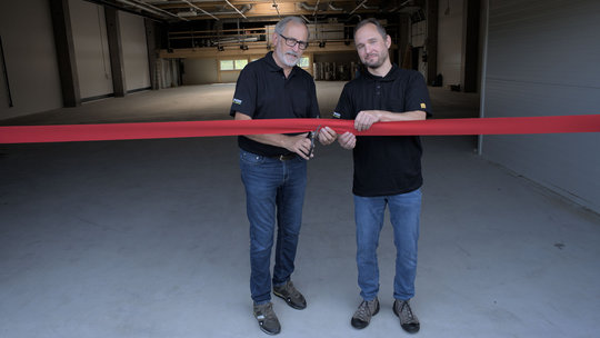
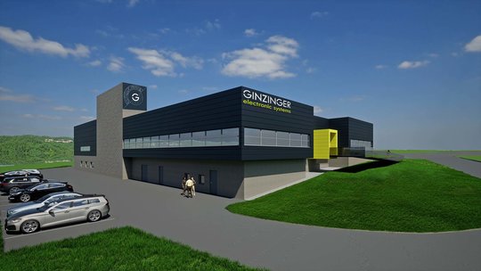
Opening of Ginzinger's new building
Due to the very pleasing order situation, an additional production hall was built at Ginzinger electronic systems in Weng im Innkreis in the first half of 2022. The ceremonial inauguration took place on Friday, July 22, 2022.

![[Translate to Englisch:]](/fileadmin/_processed_/2/9/csm_Dev_Kit_schachtel_4d2cb32b4e.jpg "[Translate to Englisch:]")

![[Translate to Englisch:]](/fileadmin/_processed_/9/2/csm_sichere_software_0b9ea6b358.jpg "[Translate to Englisch:]")


![[Translate to Englisch:]](/fileadmin/_processed_/0/4/csm_futuristisch_750ab72599.jpg "[Translate to Englisch:]")
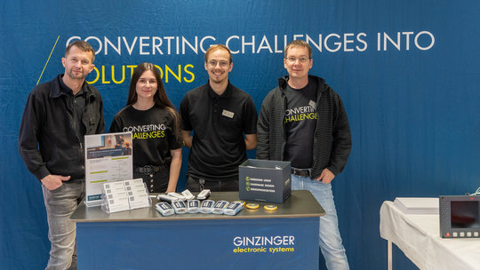
![[Translate to Englisch:]](/fileadmin/_processed_/e/5/csm_Messestand_mit_Personen_web_2399ab218b.jpg "[Translate to Englisch:]")
![[Translate to Englisch:]](/fileadmin/_processed_/2/9/csm_Dev_Kit_schachtel_a14798284a.jpg "[Translate to Englisch:]")
![[Translate to Englisch:]](/fileadmin/_processed_/4/5/csm_KI_programmiert_Software_web_be38fad3d2.jpg "[Translate to Englisch:]")
![[Translate to Englisch:]](/fileadmin/_processed_/b/6/csm_welcherweg-web_2549f701dd.jpg "[Translate to Englisch:]")
![[Translate to Englisch:]](/fileadmin/_processed_/f/c/csm_Tipps_und_Tricks_Website1900x1267-01_71e9749a93.jpg "[Translate to Englisch:]")
![[Translate to Englisch:]](/fileadmin/_processed_/9/0/csm_Cyber_Security_cfcf377b0f.jpeg "[Translate to Englisch:]")
![[Translate to Englisch:]](/fileadmin/_processed_/6/0/csm_WEG2600x-100_c7930900b1.jpg "[Translate to Englisch:]")


![[Translate to Englisch:]](/fileadmin/_processed_/c/9/csm_osadl_bild_d2855cc538.jpg "[Translate to Englisch:]")
![[Translate to Englisch:]](/fileadmin/_processed_/b/f/csm_Stefan_im_Gespraech_ohne_Mouser-web_2715b3efba.jpg "[Translate to Englisch:]")

![[Translate to Englisch:]](/fileadmin/_processed_/e/4/csm_programmieren-software-1600x900_fcf92b213a.jpg "[Translate to Englisch:]")


![[Translate to Englisch:]](/fileadmin/_processed_/c/0/csm_lagerlift5_1a7556bdfa.jpg "[Translate to Englisch:]")


![[Translate to Englisch:]](/fileadmin/_processed_/c/7/csm_elektronen_d737b21fd3.jpg "[Translate to Englisch:]")


![[Translate to Englisch:]](/fileadmin/_processed_/4/3/csm_linz-web_f44ff09273.jpg "[Translate to Englisch:]")

![[Translate to Englisch:]](/fileadmin/_processed_/5/5/csm_imx8devkit-neu_54e4a0144c.jpg "[Translate to Englisch:]")
![[Translate to Englisch:]](/fileadmin/_processed_/a/b/csm_WS-GDE_8eab7b89e3.png "[Translate to Englisch:]")


![[Translate to Englisch:]](/fileadmin/_processed_/8/3/csm_fed-verleihung-web2_0b90a28820.jpg "[Translate to Englisch:]")
![[Translate to Englisch:]](/fileadmin/_processed_/4/0/csm_1920x1080_Infoscree_webstudio_317fc093dc.jpg "[Translate to Englisch:]")
![[Translate to Englisch:]](/fileadmin/_processed_/9/8/csm_ginzinger-referenz-kreisel-rally1-web_75fbeb0eb5.jpg "[Translate to Englisch:]")

![[Translate to Englisch:]](/fileadmin/_processed_/a/4/csm_Ginzinger-referenz-vereinewirtschaft-smart-meter-adapter_836dfd0125.jpg)


![[Translate to Englisch:]](/fileadmin/_processed_/f/d/csm_baustelle_web_9a786d28c4.jpg "[Translate to Englisch:]")