Production Technology at its Best. We Invest in Precision, Quality and Performance.
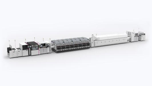
With one of the most modern machine parks, we offer you new orders of magnitude in precision, quality and throughput in EMS services. Constantly increasing demands from industry and end customers have prompted us to make the largest investment in the company's history - in our new production line. Consisting of several subsystems, we have created a production line that is second to none.
Electronic Manufacturing Services

Throughput and Precision
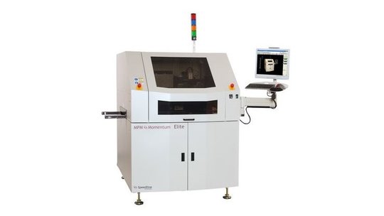
SMT Production Line
Measured and tested
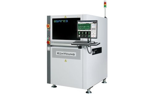
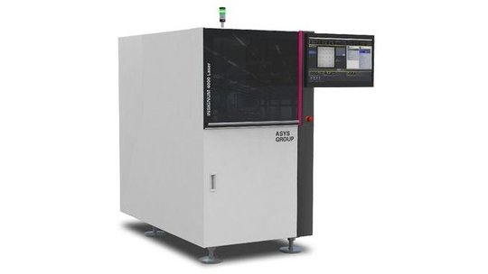
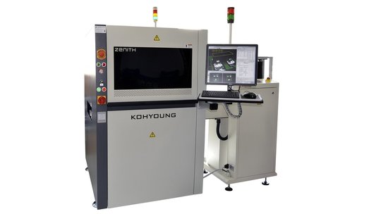
AOI - Automatic Optical Inspection
After the soldering process, the electronic assembly is measured in the AOI using a 3D measuring process. If a defect is suspected, the affected assembly is ejected for further inspection and rework. The following parameters can be automatically checked and measured:
- Solder meniscus, soldering
- Polarity of components
- Coplanarity of component and printed circuit board
- Alignment of components
- Short circuits due to soldering defects
Highlights of the AOI system at Ginzinger:
- Precise 3D measurement with 2µm resolution
- Complete inspection of all components and solder joints
- Inspection of coplanarity, tin volume and other quality features
- Feedback with the entire production line
- Massive reduction of manual post inspection
FAQ's to the 3D AOI
Why does AOI detect more than a traditional visual inspection?
3D-AOI measures every visible solder joint and component in three dimensions and objectively. This results in verifiable quality rather than subjective visual assessments. Defects are detected more quickly, reliably, and consistently. This improves functionality and service life while reducing customer complaints.
What exactly does the 3D AOI system measure at Ginzinger?
First, it checks whether all components are present. It also verifies their size, position, and offset. Optionally, coplanarity or markings can also be checked. In addition, the AOI inspects all visible solder joints. Depending on the geometry, 2D, 3D, or combined inspection methods are used for this purpose.
Can AOI actively support process optimization?
Yes, AOI detects drift trends before defects occur. This allows processes to be adjusted more quickly and helps prevent failures in downstream inspections or in the field.
How small can components be for AOI measurement?
In theory, chip sizes starting at 008004 (0.25 x 0.125 mm) can be inspected. This makes AOI well-suited for the miniaturization of the future. In practice, robust and efficient inspections have proven effective for chip sizes starting at 0402. This is because the smaller the components, the more complex the parameterization becomes, and false detections occur more frequently.
Does AOI also protect against field failures?
Yes. AOI detects missing, misaligned, or lifted components, as well as inadequate solder joints, at an early stage. This reduces the risk of hidden defects and subsequent equipment failures, which in turn reduces customer complaints and safeguards product quality.
How does 3D AOI differ from 2D systems?
3D-AOI measures components and solder joints volumetrically rather than relying solely on grayscale images. This allows for much more precise detection of heights, shapes, and complex contours. Simply put: 2D sees a silhouette, while 3D sees the entire structure. In addition, a 3D system can also perform traditional 2D analyses.
What are the benefits of AOI for new products?
The 3D AOI system provides objective feedback on component placement and soldering, particularly during prototype and initial production runs. As a result, new products achieve a consistent level of quality more quickly and can be brought into mass production with greater confidence.
Does AOI support documentation, traceability, and audit readiness?
Yes. The system can document inspection points, including measurement values and images. This makes it possible to verify that assemblies are manufactured in accordance with specifications. This is particularly important for industries such as automotive, medical technology, and manufacturing. However, it is important to note the high storage requirements: The long-term archiving of large amounts of data incurs additional costs.
Does AOI make my product more expensive?
Although AOI incurs additional inspection costs, it simultaneously reduces rework, scrap, manual visual inspections, and field complaints. In many applications, the cost of inspection is therefore quickly recouped and helps ensure consistently high product quality.
Is 3D-AOI even suitable for our production volumes?
Yes. Today, a basic test program for new assemblies can be created with the help of AI. Existing test programs and empirical data can also be reused. This makes it cost-effective to test even small quantities and prototype runs.
How do you make life difficult for an AOI system?
Challenging inspection conditions arise where visual contrasts are low. For example, on black components on black solder resist or on highly reflective surfaces. Very high component densities that cause shading also make inspection more difficult.
What are the limits of AOI?
AOI can only inspect what is visually visible. Hidden solder joints—such as those found in BGAs or LGAs—can only be inspected to a limited extent, if at all. Furthermore, the inspection limits depend heavily on the layout, package density, component geometry, and PCB design. The goal is always to find the optimal balance between high defect detection and as few false positives as possible.
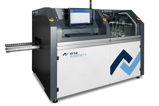
Fully Automated Soldering
In order to solder THT components quickly, fully automated and in highest precision, a selective soldering system can be used. The ECOSELECT 4 from Kurtz Ersa is ideally suited for small to medium-sized series where flexibility is paramount. The machine has a high-quality, continuous roller transport system and is equipped with power convection. This ensures optimum homogeneous heating even for the most difficult components. A programmable precision spray fluxer with integrated spray jet control ensures the precise and economical application of flux, both in single spots and in entire paths.
A configurable double-seal system makes it possible to work simultaneously with two different supplies and with solder nozzles of different diameters. Connector strips, for example, can be soldered quickly with a large-diameter nozzle, while solder joints that are difficult to access can be soldered with a very narrow solder nozzle.
Highlights of our selective soldering system:
- Flexibly integrable soldering system: inline and batch operation
- PCB mounting 508x508 mm
- up to two spray heads
- up to two stocking systems
- Power convection
- double crucible y/z-variable
- automatic nozzle activation
- extension to full inline machine by independent flux module
- Automatic measurement of solder wave height
Precisely separated
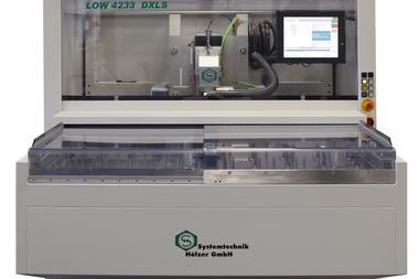
Depanelizer
With the LOW4233XL laser depaneling machine, rigid and flexible printed circuit boards can be separated automatically and precisely. Different materials and thicknesses are separated with reproducible high cut quality, low stress and low dust. Sensitive components are protected. Image-supported teach-in programming ensures automatic position correction in the depanelizer and maximum precision.
Highlights of the depaneling system:
- UV nanosecond laser
- Possibility of separating pre-milled aluminum circuit boards
- Cutter breakage control
- Flexible pick-up systems for the PCB blank
- Air ionization
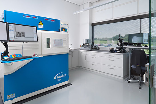
We have the insight
X-ray System
With the Nordson Dage Quadra 7, Ginzinger electronic systems has one of the most modern X-ray analysis systems. Electronic assemblies with BGAs and LGAs can be analyzed with regard to solder quality.
Potential weak points are immediately detected thanks to high-quality X-ray images and computer tomography. Whether component positioning, possibly existing voidings in the solder joint, or short circuits between the potentials. Using an X-ray detector, images can be taken with a 6.7 megapixel camera and 0.1 μm resolution.
Tomosyntheses or complete µCT images are obtained in a short time. The 3D inspection enables detailed sectional or layered images of electronic assemblies and components. For multilayer printed circuit boards, specific planes, fractures or cracks can be viewed. Molded components can be inspected, as well as relevant solder joints with regard to fill level and other quality characteristics.
Ginzinger electronic systems also offers X-ray analysis as a service for industries outside of electronics.
Extensive test procedures
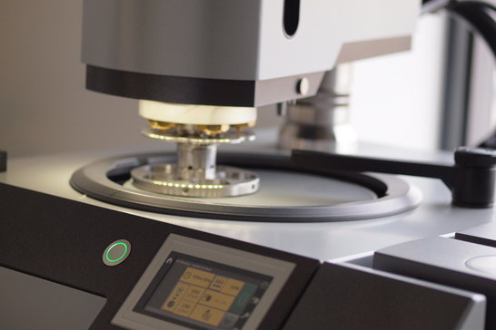
Metallurgy Lab
The metallurgy laboratory at Ginzinger electronic systems has numerous capabilities for in-depth destructive testing of solder joints, vias and copper layer thicknesses.
The inventory list includes:
- a grinding-polishing machine for metallographic preparation
- a cutting machine
- a high-resolution microscope with 2000x magnification
- a universal testing device for tensile and compression tests according to EN62137-1-2.